NE555 SA555 - SE555 GENERAL PURPOSE SINGLE "bipolar" TIMERS
# DESCRIPTION
 # DESCRIPTION
Quote: Datasheet
Quote:LMC555 CMOSタイマ
The NE555 monolithic timing circuit is a highly stable controller capable of producing accurate time delays or oscillation. In the time delay mode of operation, the time is precisely controlled by one external resistor and capacitor. For a stable operation as an oscillator, the free running frequency and the duty cycle are both accurately controlled with two external resistors and one capacitor. The circuit may be triggered and reset on falling waveforms, and the output structure can source or sink up to 200mA
LOW TURN OFF TIME
MAXIMUM OPERATING FREQUENCY GREATER THAN 500kHz
TIMING FROM MICROSECONDS TO HOURS
OPERATES IN BOTH ASTABLE AND MONOSTABLE MODES
HIGH OUTPUT CURRENT CAN SOURCE OR SINK 200mA
ADJUSTABLE DUTY CYCLE
TTL COMPATIBLE
TEMPERATURE STABILITY OF 0.005% PER°C
APPLICATION INFORMATION
MONOSTABLE OPERATION
In the monostable mode, the timer functions as a one-shot. Referring to figure 10 the external capacitor is initially held discharged by a transistor inside the timer

The circuit triggers on a negative-going input signal when the level reaches 1/3 VCC. Once triggered, the circuit remains in this state until the set time has elapsed, even if it is triggered again during this interval. The duration of the output HIGH state is given by t = 1.1 R1C1 and is easily determined by figure 12.

Notice that since the charge rate and the threshold level of the comparator are both directly proportional to supply voltage, the timing interval is independent of supply. Applying a negative pulse simultaneously to the reset terminal (pin 4) and the trigger terminal (pin 2) during the timing cycle discharges the external capacitor and causes the cycle to start over. The timing cycle now starts on the positive edge of the reset pulse. During the time the reset pulse in applied, the output is driven to its LOW state.
When a negative trigger pulse is applied to pin 2, the flip-flop is set, releasing the short circuit across the external capacitor and driving the output HIGH. The voltage across the capacitor increases exponentially with the time constant t = R1C1. When the voltage across the capacitor equals 2/3 VCC, the comparator resets the flip-flop which then discharge the capacitor rapidly and drivers the output to its LOW state.
Figure 11 shows the actual waveforms generated in this mode of operation.
When Reset is not used, it should be tied high to avoid any possibly or false triggering.
ASTABLE OPERATION

When the circuit is connected as shown in figure 13 (pin 2 and 6 connected) it triggers itself and free runs as a multi vibrator. The external capacitor charges through R1 and R2 and discharges through R2 only. Thus the duty cycle may be precisely set by the ratio of these two resistors. In the astable mode of operation, C1 charges and discharges between 1/3 VCC and 2/3 VCC. As in the triggered mode, the charge and discharge times and therefore frequency are independent of the supply voltage.

Figure 14 shows actual waveforms generated in this mode of operation. The charge time (output HIGH) is given by: $$t1 = 0.693 (R_1 + R_2) C_1$$ and the discharge time (output LOW) by: $$t2 = 0.693 (R_2) C_1$$ Thus the total period T is given by: $$T = t1 + t2 = 0.693 (R_1 + 2R_2) C_1$$ The frequency of oscillation is then: $$f = \frac{1}{T}= \frac{1.44}{(R_1+2R_2)C_1}$$ may be easily found by figure 15.

The duty cycle is given by: $$D = \frac{R_2}{R_1+ 2R_2}$$
PULSE WIDTH MODULATOR
When the timer is connected in the monostable mode and triggered with a continuous pulse train, the output pulse width can be modulated by a signal applied to pin 5. Figure 16 shows the circuit.

LINEAR RAMP
When the pull-up resistor, RA, in the monostable circuit is replaced by a constant current source, a linear ramp is generated. Figure 17 shows a circuit configuration that will perform this function.


Figure 18 shows waveforms generator by the linear ramp. The time interval is given by: $$ T = \frac{\cfrac{2}{3} V_{CC} \times R_E (R1+R2) C}{R_1 V_{CC} - V_{BE} (R_1+R_2)} $$ $$ V_{BE} = 0.6V$$
50% DUTY CYCLE OSCILLATOR
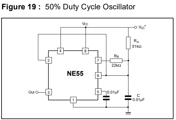
For a 50% duty cycle the resistors $R_A and R_E$ may be connected as in figure 19. The time period for the output high is the same as previous, $$t1 = 0.693 R_A C$$ For the output low it is t2 $$t2 =\frac{R_A \times R_B}{R_A + R_B} C \times Ln \left( \frac{R_B – 2R_A}{2R_B - R_A} \right) $$ Thus the frequency of oscillation is: $$f = \frac{1}{t1 + t2}$$
Note that this circuit will not oscillate if RB is greater than 1/2 RA because the junction of RA and RB cannot bring pin 2 down to 1/3 VCC and trigger the lower comparator.